Scanning Electron Microscopy (SEM)
Scanning Electron Microscopy (SEM) uses a beam of electrons to image at a sub-micron resolution – much higher than is possible with an optical microscope. The electron beam interacts with the atoms in the sample and causes several different signals to be emitted. This allows High resolution SEM images to be combined with elemental mapping using Energy Dispersive X-ray spectroscopy (EDX) or with crystal grain orientation and boundary mapping using Electron Backscatter Diffraction (EBSD).
Contact
Instrument Leader: Professor Sarah Harmer
SEM Facility Manager: Dr Alexander Sibley

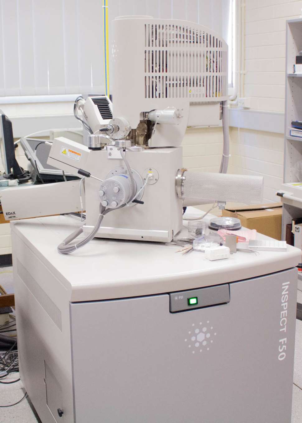
FEI Inspect F50 Field Emission SEM
- Secondary Electron detector
- Backscatter Electron detector
- Amated EDAX EDS detector
- EDAX EBSD detector
Sample coating facility also available
- Emitech K75X single Target sputter coater
- Quorumtech Dual Target sputter Coater
- Cressington 208HR Sputter coater
- Cressington 208C carbon coater
Samples must be solid, dry, conductive (facility available for surface coating). Sample size up to 100mm x and y, 40mm z
Application examples

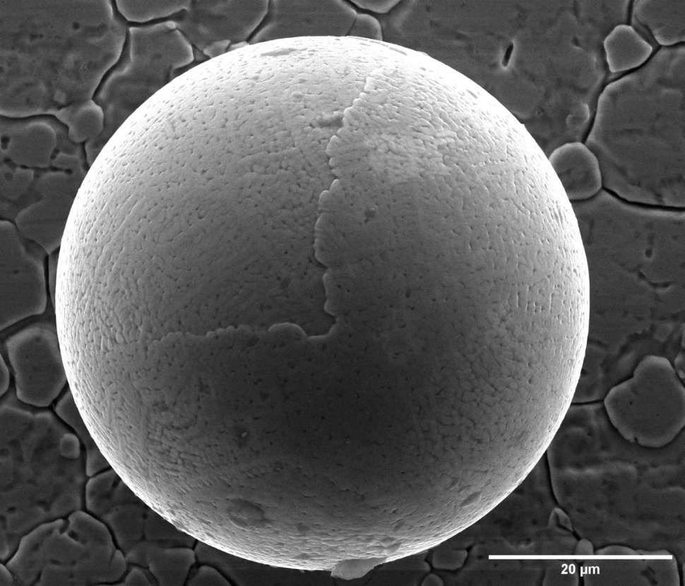
SEM image of a steel particle on a polished steel surface. The grain structure of the steel can be seen in the background, while the particle itself has it’s own microstructure.

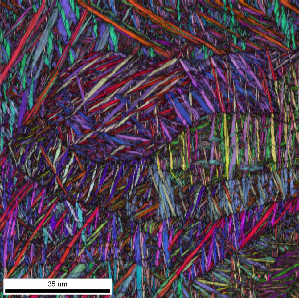
EBSD Map of a polished titanium oxide surface – different colours show different orientations of the crystal structure
Our equipment is funded by:


![]()
Sturt Rd, Bedford Park
South Australia 5042
South Australia | Northern Territory
Global | Online
CRICOS Provider: 00114A TEQSA Provider ID: PRV12097 TEQSA category: Australian University


